In modern electronics, printed circuit boards (PCBs) are the foundation for numerous devices, from smartphones to medical equipment. To bring these intricate boards to life, manufacturers employ various cutting-edge technologies. One such technology is the Laser Direct Imaging (LDI) unit, a vital tool in the PCB manufacturing process. In this blog post, we will delve into the fascinating world of LDI units and explore how they revolutionize the creation of circuit boards.
What is Laser Direct Imaging?
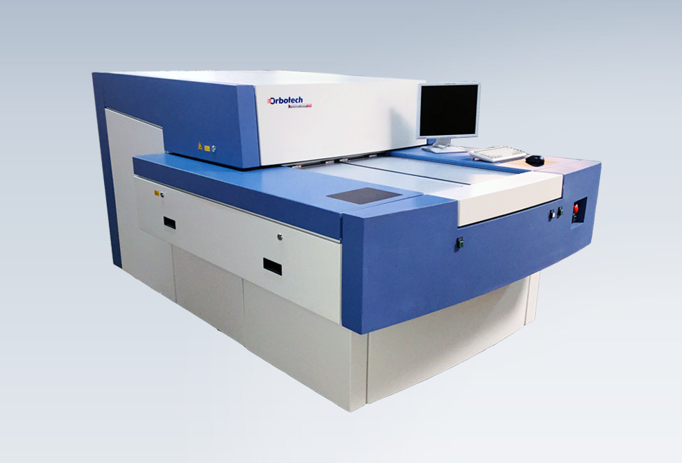
Laser Direct Imaging, often called LDI, is an advanced technique used in PCB manufacturing. Traditionally, the process involved using a photomask, a physical stencil that transferred the circuit pattern onto a photosensitive layer of the board. However, LDI units have replaced this method by utilizing lasers to expose the board directly.
The LDI Process:
1. Preparation of PCB: The process begins with preparing the PCB substrate. A photosensitive material, known as a dry film or solder mask, is applied to the board’s surface. This material is designed to harden when exposed to ultraviolet (UV) light.
2. Digital Data Input: The circuit board design is converted into a digital format compatible with the LDI unit. This digital data is typically in the form of Gerber files, which contain all the necessary information regarding the circuit layout.
3. Alignment and Registration: The PCB is loaded into the LDI unit, which uses a combination of optical systems and computer algorithms to align and register the board precisely. This alignment ensures that the laser will expose the correct areas on the board.
4. Laser Exposure: The LDI unit activates a high-resolution laser once the alignment is complete. This laser moves across the board’s surface, selectively exposing the photosensitive material based on the digital data received. The laser quickly scans the board, providing precise and accurate imaging.
5. Development and Etching: After the laser exposure, the board develops. This process removes the unexposed photosensitive material, leaving only the desired circuit pattern. The board is then subjected to etching, where chemicals remove the exposed copper and create the necessary circuit traces.
6. Finishing Touches: Once the circuit traces are etched onto the board, other processes, such as solder mask application, surface finish, and component assembly, take place to complete the PCB manufacturing process.
Advantages of LDI Units:
1. Increased Precision: LDI units offer higher precision than traditional photomask methods. The laser can accurately expose fine features and intricate circuit patterns, improving circuit board performance.
2. Time and Cost Efficiency: LDI eliminates the need for photomasks, which can be time-consuming and expensive. The digital nature of LDI allows for faster design iterations and reduced setup times, resulting in more efficient production cycles.
3. High Resolution and Yield: LDI units enable high-resolution imaging, which ensures the accurate reproduction of complex circuit designs. This precision reduces the chances of manufacturing defects and increases overall production yield.
Laser Direct Imaging units have become an indispensable part of the PCB manufacturing process, revolutionizing how circuit boards are produced. By leveraging advanced laser technology and digital data, LDI units provide increased precision, time and cost efficiency, and higher production yields. As the electronics industry evolves, LDI units will undoubtedly play a crucial role in meeting the demand for smaller, faster, and more intricate PCBs.
Leave a Reply